Week 8: Electronics Production
In this week's group work Antti taught us how to manafacture PCB's through milling. This was my first time ever seeing a PCB being milled and it was quite fun to see.
PCB Production
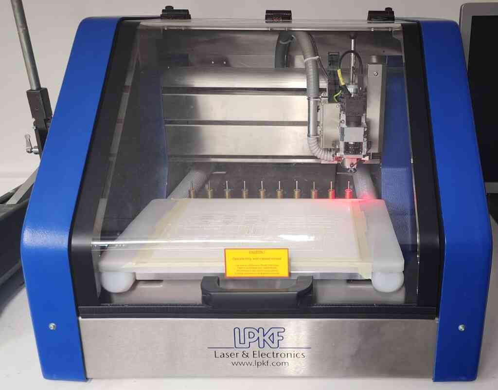
We had a LPKF milling machine for producing PCB's here at the FAB lab Oulu which I used to mill my PCB.
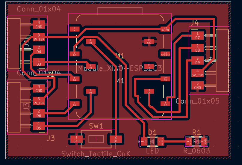
First I extracted my gerber files from kicad for my design.
Then I went to the Lpkf machine and turned it on and opened the software on the computer.
.png)
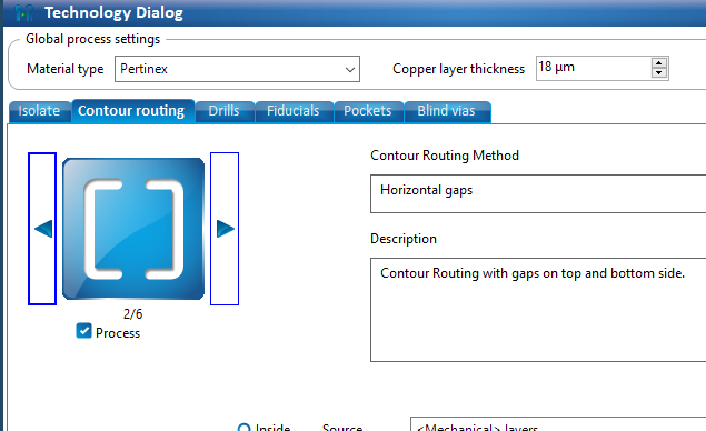
After that I used the default template and went to the process planning wizard on the top toolbar.
.png)
There I selected all the options I needed for my PCB.
.png)
.png)
.png)
After that I imported my files into the software. Then I went to isolate and generate Contours so I can easily remove the PCB once its milled and cut.
.png)
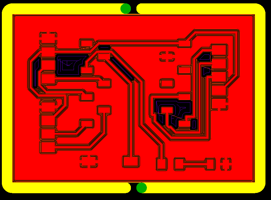
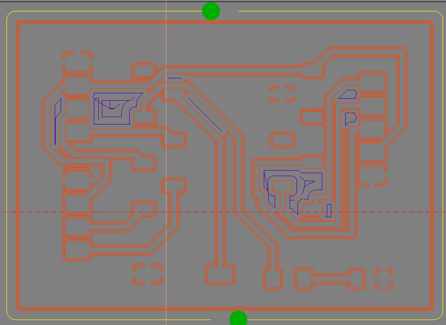
Once that was done it generated the PCB with the toolpaths and everything.
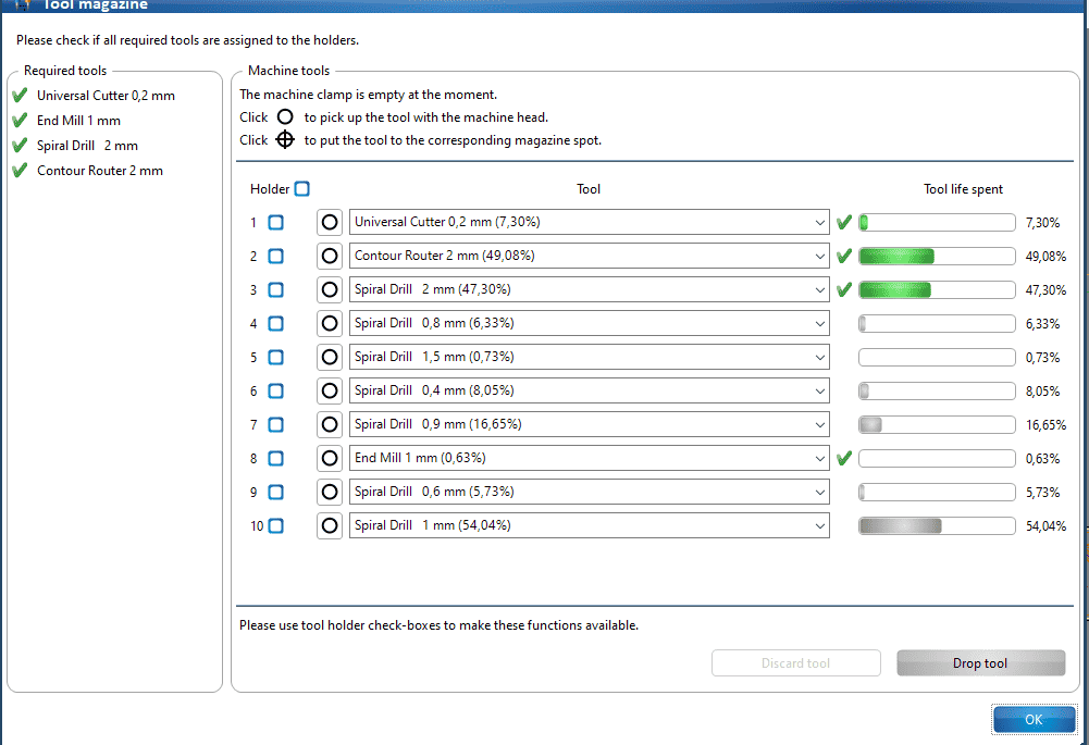
Then I went to the toolbar and checked if all the tools were alright, which they were.
Then finally I went to the board production wizard.
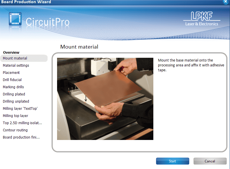
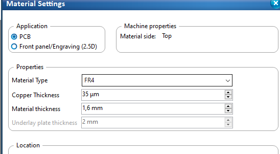
Then I taped the FR1 material I was using. I found out with Antti that for some reason if you selected FR1 in the materials it didn't have the correct toolpaths for it so we just went with FR4.
.jpg)
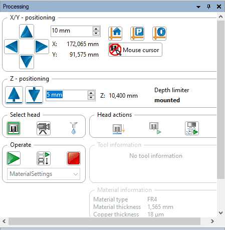
Afterwards, I inputted the materials measurements and made the area where I wanted my PCB cut using p1 and p2
For accurate placement you can use the keys to position the drill head.
Then it asked me if I wanted any copies of the design.
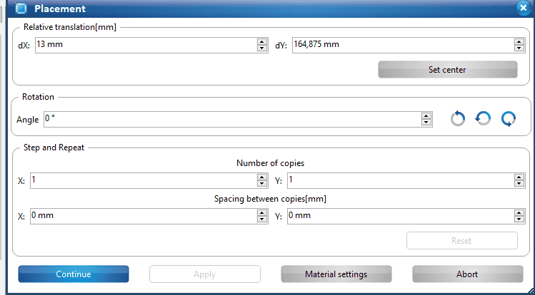
Lastly, It adjusted the focal height itself and asked me If it was okay, which I checked again by milling a line and then using a point to point measurement to see if the distance was close 0.2mm which is acceptable. Finally, it started milling.
Here Is a video of it milling.
After it was done milling I removed the PCB and cleaned it up a bit using IPA and srubbing pad.
.jpg)
Solder Mask
I wanted to apply a cool solder mask to my pcb so I found a dedsec image online and imported it to inkscape. I also went to kicad and plot where I exported svg files of the edge cuts and front copper layer
Afterwards, Imported the svg file into inkscape converted the edge cut file to path and then used set clip so image can fit the area and avoid the copper pads.
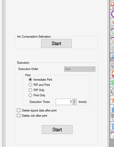
Then I exported the file as a pdf and went to the UV printer.
First I set the origin and printed the rectangle area where I would place my PCB.
.jpg)
Then on top of it I placed my PCB making sure it fit properly and wasn't misaligned. Then I went to the computer and I applied a spcial plating to my pdf design so It would do a white ink layer first so everything sticks better.
Then I sent it for printing.
This is the final result after the UV printing.
.jpg)
Soldering
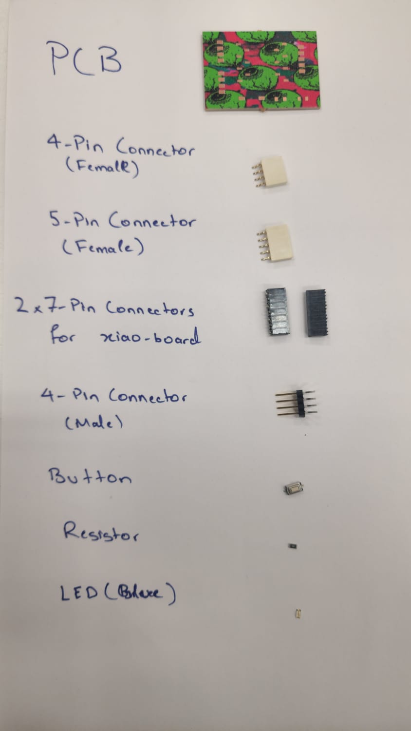
I first gathered all the components I would need in one place.
Then I soldered the components one by one. Here is where some stuff went wrong. In my first PCB that I produced and soldered the soldering was bad as I have almost no experience in soldering so when I tested the board it wasn't working properly and the nail in the coffin was one of the xiao connectors came of with the pad which just meant it was kinda dead and time for a new one. I made a new PCB using all the above steps and then did the soldering again much better this time.
.jpg)
Here is the final result of the soldered PCB.
.jpg)
 (1).jpg)
Testing
After I was done soldering I connected the PCB to my computer and uploaded the code I had written for it. The code was a simple code that made the LED go On and off with the button .
#define BUTTON_PIN D1  // D1 = GPIO1
#define LED_PIN    D2  // D2 = GPIO2

void setup() {
  pinMode(LED_PIN, OUTPUT);
  pinMode(BUTTON_PIN, INPUT_PULLUP);  // Internal pull-up makes it HIGH when not pressed
}

void loop() {
  int buttonState = digitalRead(BUTTON_PIN);

if (buttonState == HIGH) {
    // Button NOT pressed → Pin is pulled HIGH by internal resistor → LED ON
    digitalWrite(LED_PIN, HIGH);
  } else {
    // Button IS pressed → Pin is connected to Ground (LOW) → LED OFF
    digitalWrite(LED_PIN, LOW);
  }
}
After uploading the code I tested it and it worked perfectly. The LED turned off when I pressed the button and remained on due to the input_pullup which kept the state high when button was not pressed.
Here is a video of the testing.
I then tested each pin with a wire and multimeter to see if they were working and there were no issues there, which they were non off thankfully.
.jpg)
So everything was working fine in the PCB and here is the image of it with the LED on.
.jpg)
Overall, this week was quite fun and I actually really enjoyed producing the PCB's, then learning better soldering and my favourite part was the soldermask I applied to the PCB.
Download File
 ← Back to Main Page